Key Words: Silicon Wafer Dicing PCB Depaneling Glass Cutting
Home > News > Industry News
【Description】:
Discover UV laser via drilling solutions for automotive-grade LTCC substrates.
At 77 GHz, the wavelength in LTCC (Dk ≈ 6) is approximately 1.7 mm. Every via in the RF path introduces parasitic inductance and capacitance that can degrade signal integrity, increase insertion loss, and detune antenna arrays. To minimise these effects, vias must be:
Small: 50–75 μm diameter for RF transitions.
Precisely placed: ±20 μm positional accuracy to maintain phase coherence across antenna arrays.
Clean‑walled: No debris, recast, or excessive taper that would alter impedance.
Reliable: Consistent resistance (<10 mΩ) and no micro‑cracks.
Mechanical punching cannot achieve these requirements at the 50–75 μm scale. UV laser drilling has therefore become the standard method for 77 GHz radar LTCC substrates.
The 355 nm UV wavelength is strongly absorbed by the organic binders in LTCC green tape, enabling clean, photochemical ablation with minimal thermal damage. Key advantages for radar substrates include:
Fine via diameters: Down to 30 μm with excellent roundness.
High positional accuracy: Galvo scanners with vision alignment achieve ±20 μm.
Post‑lamination drilling: For multilayer radar substrates (8–12 layers), drilling after lamination ensures perfect layer‑to‑layer registration—critical for RF signal integrity.
Minimal HAZ: Nanosecond UV lasers limit the heat‑affected zone to 10–20 μm; picosecond lasers reduce it to <5 μm.
Power electronics—traction inverters, on‑board chargers, DC‑DC converters—require LTCC substrates that can conduct heat away from dies and carry high currents. Thermal via arrays are the primary solution: hundreds or thousands of vias, 100–200 μm in diameter, filled with copper or silver paste, connecting the die attach surface to an embedded heat spreader or the backside.
These vias must be:
High aspect ratio: Substrate thickness of 500–1000 μm requires aspect ratios of 3:1 to 5:1.
Dense: Via pitch as small as 300 μm.
Clean: Any debris or recast on the via walls prevents complete paste filling, leading to voids and hot spots.
UV laser drilling with multi‑pass or helical strategies is used to achieve high aspect ratios without excessive taper. Key parameters:
Helical drilling: 4–6 revolutions, 20–30 μm pitch, 800 mm/s scan speed.
Skip‑drilling: Drill vias in a non‑sequential order to allow heat dissipation in dense arrays.
Pulse energy: 30–50 μJ for 150 μm vias in 800 μm thick tape.
Focus: Dynamic focus adjustment maintains beam position as depth increases.
After drilling, a low‑energy clean‑up pass removes loosely adhered debris, followed by ultrasonic or plasma cleaning. Via walls are then inspected by SEM to confirm the absence of recast.
Beyond via drilling, laser processing is used for:
Cavities: For die placement, laser milling creates recesses in the green tape stack with precise depth control (±10 μm).
Edge trimming: Laser cutting defines the final substrate outline, eliminating mechanical dicing and its associated chipping.
These processes are typically performed on the same laser platform, reducing handling and alignment errors.
Automotive‑grade LTCC substrates must satisfy AEC‑Q200 and be manufactured under IATF 16949. Laser processing contributes to these requirements in several ways:
Laser drilling systems with real‑time monitoring and statistical process control ensure that via diameter and position meet Cpk targets. For example, a via diameter of 75 ± 5 μm can be maintained with Cpk > 2.0.
Every via’s drilling parameters (pulse energy, repetition rate, focus position, gas flow) are logged and linked to the substrate serial number. This data supports root‑cause analysis and continuous improvement.
In‑process gas assist and post‑process cleaning eliminate debris that could cause via voids or electrical shorts. HAZ control (<15 μm for nanosecond, <5 μm for picosecond) preserves the dielectric properties and mechanical strength of the LTCC, ensuring reliability under thermal cycling and vibration.
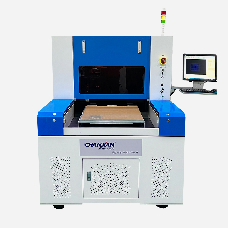
Chanxan Laser offers a comprehensive range of UV nanosecond and picosecond laser systems purpose‑built for automotive‑grade LTCC green tape processing. Our solutions address the specific demands of 77 GHz radar and power electronics packaging.
Whether you are producing radar modules for ADAS or power substrates for EV inverters, Chanxan Laser provides the technology and expertise to meet your production targets.
| Free solution
Previous: Laser Processing for 5G/6G LTCC: RF Modules & Antenna‑in‑Package
Next: LTCC Laser Via Drilling: A Practical Troubleshooting Guide for HAZ Reduction and Clean Via Walls